|
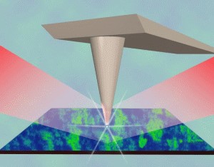
Fig.1. The infrared nanoscope employs an AFM whose
tip concentrates the infrared illumination to an extraordinarily
fine focus of only 20 nm diameter. Scattered infrared light is
recorded to obtain an ultra-resolved infrared image, here of metal
puddles in VO2.
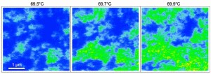
Fig.2. Infrared snapshot images taken during the
critical temperature range of the Mott transition of VO2. The
transition from insulator to metal clearly proceeds by
temperature-induced growth and coalescence of initially separate
metal puddles.
Images � by
MPI of Biochemistry
|
Materials such as copper metal contain
electrons that are mobile enough to conduct an electrical current. In
conducting materials such as copper, gold, silver, or aluminum,
electrons do not hinder one another and are free to move about the
lattice structure of the material. In more-complex crystal oxides,
such as vanadium dioxide, electrons can become influenced by nearby
positively or negatively charged particles, and their movement can
become hindered. These materials are known by physicists as "correlated
materials."
Correlated materials include superconductors or
semiconductors-crystals peppered or "doped" with atoms that may donate
mobile electrons to the solid. Correlated materials can exhibit
extraordinary changes in their physical properties, such as
transforming from an insulating material to a conducting material,
when subjected to relatively small changes in pressure or temperature.
Vanadium dioxide begins becoming conductive when reaching 68�C, and is
fully metallic already at 71�C. On cooling the conductivity disappears.
For decades scientists have puzzled over how this transformation to a
fully metallic state - known as "Mott"
metal-insulator transition - occurs.
Condensed-matter spectroscopist D.N. Basov and theorist A.V. Balatsky
argued that the transition begins when tiny metallic puddles begin
forming at sites of impurities or imperfections within the lattice,
and looked out how to make such puddles visible by some sort of "nanoscale
viewer".
The infrared nanoscope developed in the lab of F. Keilmann offered a
fitting solution. This instrument had already yielded widely
recognized results. Recently it enabled infrared spectral inspection
of single viruses of below 20 nm thickness (a human hair is 80 000 nm
thick) or of modern transistors of 65 nm size. D.N. Basov set out to
visit Martinsried for a successful study of Korean-prepared and
characterized VO2 crystals. M. Brehm, then postdoc,
observed the initially structureless, flat crystal becoming, in the
critical temperature region, full of tiny metal inclusions that grew
and finally coalesced. These infrared nanoscope images have revealed
for the first time a new type of metal "phase" characterized by
unusually strong electron correlation existing only during the
transition of the material from its insulating state to its conducting
state.
The infrared nanoscope works at long wavelength of 10 000 nm. It is
capable of resolving these tiny objects only because its light is
virtually fine-focused by the AFM's probing tip. This mechanism is
akin to how an automobile antenna concentrates radio waves into the
receiver. The metal puddles highly reflect the infrared nano-focus and
thus become highlighted in the image.
The new findings will help researchers worldwide better describe and
understand underlying physical laws of how charges propagate through
correlated materials. The research could help
materials scientist understand how to precisely dope a material with
specific atoms in order to optimize conducting or superconducting
behaviour or, conversely, to create materials impervious to electrical
conductivity or magnetic influences.
"What is extremely exciting about this research
is that four different laboratories with complementary disciplines
cooperated to use this infrared nanoscope in its first successful
application for solving a solid-state physics puzzle," Keilmann said.
|