|
Current News |
|
Chemistry A to Z |
|
About Internetchemistry |
|
- Imprint |
|
|
Modified electron microscope identifies atoms |
|
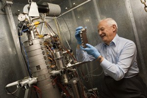
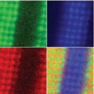
A new electron microscope recently installed in Cornell's Duffield Hall is enabling scientists for the first time to form images that uniquely identify individual atoms in a crystal and see how those atoms bond to one another. And in living color. "The current generation of electron microscopes can be thought of as expensive black and white cameras where different atoms appear as different shades of gray," explained David Muller, Cornell associate professor of applied and engineering physics. "This microscope takes color pictures - where each colored atom represents a uniquely identified chemical species." |
|
The instrument is a new type of scanning transmission electron microscope (STEM), built by the NION Company of Kirkland, Wash., under an instrument-development award to Cornell from the National Science Foundation (NSF). John Silcox, the David E. Burr Professor of Engineering at Cornell, and Ondrej Krivanek of NION are co-principal investigators on the project. The microscope incorporates new aberration-correction technology designed by Krivanek that focuses a beam of electrons on a spot smaller than a single atom - more sharply and with greater intensity than previously possible. This allows information previously hidden in the background, or "noise," to be seen. It also provides up to a hundredfold increase in imaging speed. The capabilities of the new instrument in analyzing a test sample are described in an article in the Feb. 22, 2008, issue of the journal Science by Muller, Silcox, Krivanek and colleagues at Cornell and in Korea and Japan. It allows scientists to peer inside a material or a device and see how it is put together at the atomic scale where quantum effects dominate and everyday intuition fails. One of the most important applications of the new instrument will be to conduct what Silcox calls "materials pathology" to aid researchers in their development of new materials to use in electronic circuits, computer memories and other nanoscale devices. "We can look at structures people have built and tell them if they've built what they thought they did," Silcox explained. A STEM shoots an electron beam through a thin-film sample and scans the beam across the sample in subatomic steps. In addition to forming an image, the new microscope can identify atoms in its path by a process called electron energy-loss spectrometry. Atoms in the path of the beam absorb energy from some of its electrons to kick their own electrons into higher orbits. The amount of energy this takes is different for each kind of atom. The detector that collects electrons emerging from the sample measures the energy losses, and from this the atoms in the path of the beam can be identified. The detector can simultaneously produce multiple images -- one for every different species of atom in the sample, and these can be color-coded, each color representing a different electron energy signature. The method also can show how atoms are bonded to one another in a crystal, because the bonding creates small shifts in the energy signatures. In earlier STEMS, many electrons from the beam, including those with changed energies, were scattered at wide angles by simple collisions with atoms. The new STEM includes magnetic lenses that collect emerging electrons over a wider angle. Previously, Silcox said, about 8 percent of the emerging electrons were collected, but the new detector collects about 80 percent, allowing more accurate readings of the small changes in energy levels that reveal bonding between atoms. More complete collection and a brighter and a more sharply focused beam also allow the new microscope to scan much faster. In early tests it collected a 4,096-pixel image in about 30 seconds, 50 to 100 times faster than in conventional STEMs. To demonstrate the capability of the new instrument, Muller examined a sample consisting of layers of two different materials: lanthanum-strontium-manganese oxide and strontium-titanate. This was done as part of a research project on which he is collaborating with scientists in Korea and Japan. "It's an artificial structure that will have interesting magnetic and electrical properties," he said, "but for it to work properly we have to make atomically sharp interfaces between the layers. It's really important to know if a few atoms leaked across the interface." In the color image from the new STEM, where manganese appears red and titanium blue, a line of purple shows mixing at the edge between the two layers. "We've learned that there's room for improvement," Muller says, adding "This wasn't our best sample, but if we had put that one in it would have been a fairly boring image." The new instrument arrived at Cornell in October, and is still undergoing calibration and testing. The problems that limited electron imaging were identified as long ago as 1935, Silcox said, and ideas for overcoming them were outlined in 1947. But it was not until very recently that the engineering obstacles to putting them into practice were overcome. Largely, he said, this is because the problem required advanced computing, including computers to design the instrument, computer-controlled machinery to manufacture parts to fine tolerances, and computers to control the instrument itself. |
|
|
|
|
Related topics - search form: |
|
|

